Printed Circuit Boards are used to connect the components that make up electronic devices. PCBs are found in many appliances and are used in many industries, due to their rigidity, low cost, and ease of manufacturing.
There are many great CAD software to create PCB designs. Most of these tools are not free of charge. KiCad is free and open-source software that acts as an alternative to those costly tools. It is well suited for small to medium size projects.
Getting started with KiCad
Let’s install KiCad and get to know the user interface.
Installing KiCad
Go to KiCad official website and download the software. Follow the installation guide for your operating system.
I will be using a windows machine and KiCad V5.1.10 for this guide.
You may want to consider donating to KiCad as long as you are there.
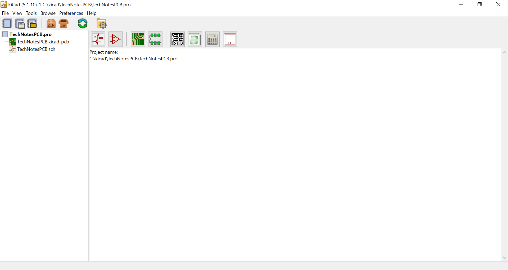
Project management window
The first window you will be presented with once you open KiCad is the project management window. This window will help you create new projects, open existing projects, manage files and folders also launch the different tools that make up KiCad.
To create a new KiCad project go to File -> New -> Project…
If you are on windows you can use CTRL + N
It is recommended to create a new empty folder for your project to keep the project files organized.
Once you are done creating the new project and giving it a cool name. You should find two new files in the left file tree window. A . sch extension file, which stands for schematics, and a . kicad_pcb extension file which is a PCB file.
PCB design is a multi-stage process, however, It can be divided into two main parts. Schematic drawing and component layout. KiCad has different tools for accomplishing the task.
KiCad Tools:
- Eeschema – Schematic layout editor
- Symbol Editor
- Pcbnew – PCB layout editor
- Footprint Editor
- GerbView – Gerber viewer
- Bitmap to Component Converter
- PCB Calculator
- Page Layout Editor
The two tools we will focus on are Eeschema and Pcbnew. They are the two main windows that you will find yourself going back and forth between. The other tools complement the functionality of Eeschema and Pcbnew.