This is part 2 of a series about PCB design with KiCad. If you missed the previous part click the link PCB Design with KiCad – Part 1
Circuit Design
Circuit design is considered the first step in PCB design. We are not going to cover circuit design principals in this series, since it is a very large topic that requires years of expertise and knowledge in electrical and electronics engineering. Of course this extends beyond the scope of this series.
If you like to learn more about circuit design, there are many great sources online, including books and courses.
The focus in this series is on the PCB design process, which mainly deals with the connectivity of the components, as well as the physical dimensions of the device. Therefore, we are going to implement well designed circuits that are proven to work. We will not concern ourselves with the electrical principals of the circuits.
In this guide I will take you through the steps to designing a 555 blinking LED circuit, which is the PCB design equivalent of “Hello World” in programming.
Eeschema
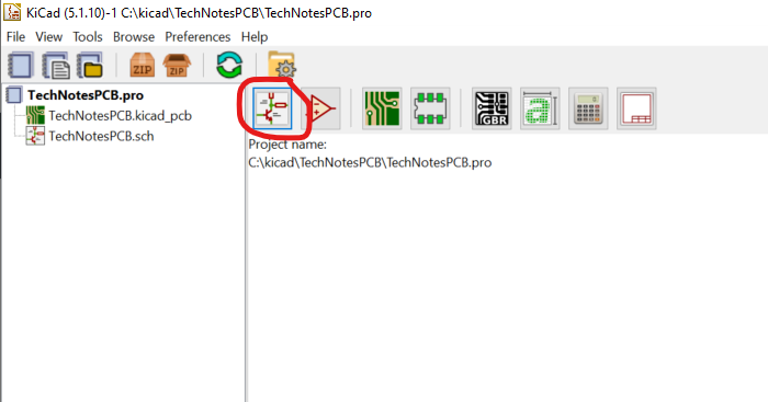
Eeschema is the schematic editor tool in KiCad. To launch the tool click on the icon as seen in the picture below.
Use the mouse to zoom in and out, and navigate around the empty schematics sheet.
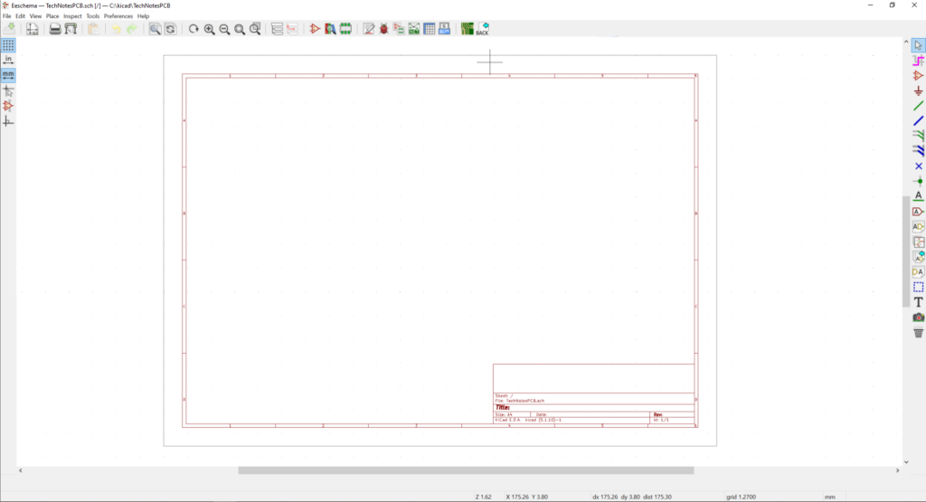
Notice, there are three toolbars, on the left, on the right and on the top.
In the schematics word components are presented as a drawing with pins and text. The schematics are basically a drawing that depicts the the connectivity of the components. The shape and size of the schematic symbol do not hold any information about the physical shape and size of the actual component, except of course the pins. Pins represent the actual electrical connectors of a component.
So why do we need schematics? Well, schematics abstract away the physical aspects of the components, and gives us the ability to annotate with numbers and text that help clarify the circuits.
In practice, the schematics of a board are consulted for information more often than the layout.
How to add components to the schematics
There are many components in the market. Usually the component manufacturer supply the designers with schematics symbols and footprint, however, this is not always the case especially for a free tool like KiCad. In that case, board designers need to create schematics symbols. We will cover that in later articles. Meanwhile, we can choose from the standard library offered by KiCad.
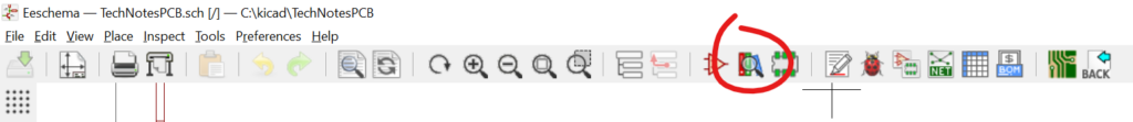
Click on the Symbol Library icon at the top toolbar.
In the Symbol Library Browser you can view the KiCad library symbols in details to see if they fit your needs.
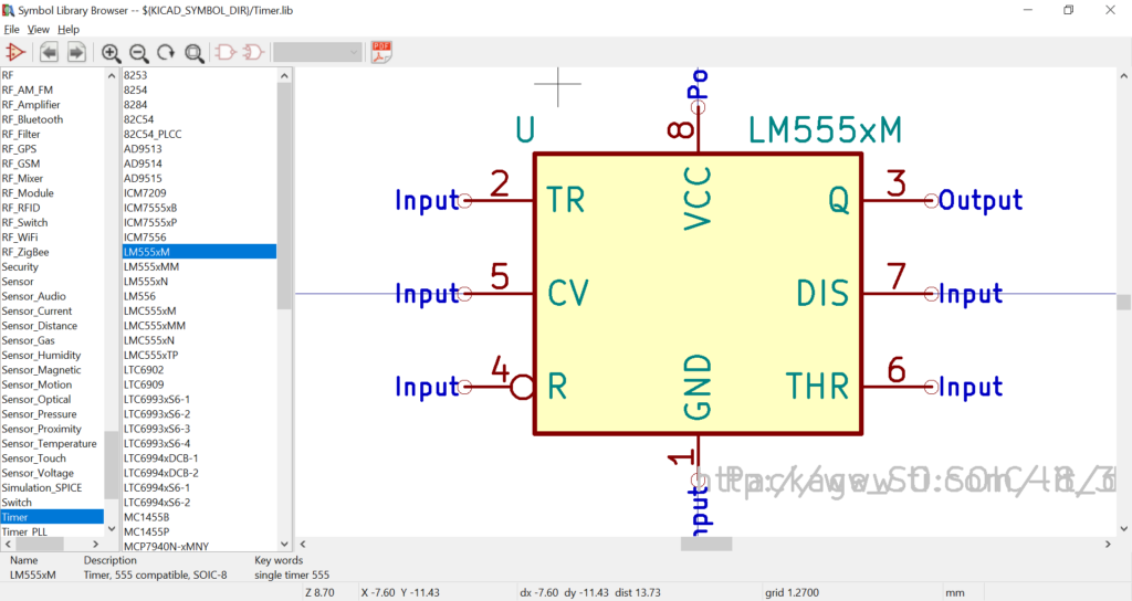
We are going to use a 555 integrated circuit timer by Texas Instruments. Datasheet
Note that in the datasheet under device information there is a table that holds information about the packaging. This information is important to us, because we want to consider the packaging of the IC when we choose a component. In our design we want to use surface-mount technology (SMT). Therefore we will pick the SOIC (8).
It is advised to consider packaging aspects at the schematics stage, even though the schematics do not represent the physical aspects of the device.
Placing symbols in the schematics
In Eeschema window click the Place Symbol icon at the right toolbar, as seen in the picture blew, and then click anywhere you want on the schematics sheet.
Another window will show up. Select Timer -> LM555xM and then click OK.
You can use the filter bar for convivence.
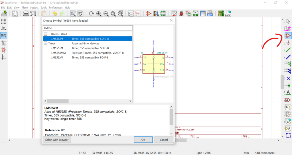
We have selected a schematics symbol for LM555 with SOIC (8) packaging. If you chose a different LM555 symbol, the design will still work, but you will have the wrong information about the packaging in your schematics.
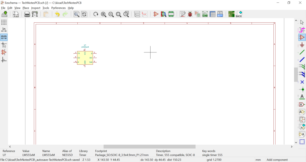
Now you can drag and place the component where you want it to be.
In the next article we will connect more components to our design.